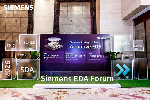
The 2026 Siemens EDA Forum was held in Shanghai. Centering on cutting‑edge technologies including AI‑empowered EDA, advanced packaging, and system‑level design and verification, the event brought together industrial‑chain enterprises, technical experts and partners to explore development directions for next‑generation electronic‑system innovation.
Ling Lin, Global Vice President and General Manager of China at Siemens EDA, stated in her opening keynote speech at the forum, “Software‑defined development, chip‑enabled capabilities and AI augmentation are jointly driving the electronics industry into a new innovation phase. Faced with ever‑rising design complexity, Siemens EDA will sharpen its focus on customer requirements, keep advancing innovations for AI‑native EDA, and work alongside Chinese customers and industry partners to boost engineering efficiency and design quality, accelerate the delivery of innovative outcomes, and seize development opportunities in the AI era.”
Ankur Gupta, Executive Vice President of the Integrated Circuits Products Division at Siemens EDA, then delivered a keynote speech titled AI‑Native Design: Shaping the Future of Chips and Systems, sharing his insights into next‑generation electronic‑design innovation paradigms. He pointed out that with the accelerated adoption of AI applications, continuous advancement of software‑defined products, and deepening heterogeneous integration, design complexity has expanded from the chip level to systems and even systems‑of‑systems. Conventional design methodologies can no longer keep pace with the fast‑moving innovation rhythm of the AI era.
According to Ankur Gupta, AI‑native design seeks to deeply embed AI across the full‑lifecycle development workflow spanning chips, packaging, circuit boards and systems. Drawing on capabilities including AI agents, GPU‑accelerated computing, comprehensive digital twins and physics‑based EDA software verification, Siemens EDA empowers engineering teams to build higher‑performance engineering engines, achieve smarter execution, and deliver trustworthy design outputs.
Beyond keynote presentations, the forum featured seven technical sub‑forums covering key domains such as custom IC design, digital front‑end and back‑end design and verification, DFT (Design‑for‑Test), advanced packaging, semiconductor manufacturing, and board‑level system design. Through technical briefings, industry practices and customer‑case exchanges, the sessions explored new pathways for electronic‑design and system innovation in the AI‑driven era.
Lincoln Lee, Global Vice President and Asia‑Pacific Technical General Manager at Siemens EDA, commented, “Against chip‑design challenges brought by AI computing, advanced process nodes, heterogeneous integration and system‑level verification, the industry demands more than faster standalone tools. It requires fundamental innovation in design methodologies to unlock engineers’ productivity at the source. Siemens EDA will continue to iterate its technical solutions and service ecosystem, helping customers effectively address these challenges and translate cutting‑edge technologies into tangible product competitiveness.”
(Reprinted from https://news.eccn.com/)