Rapidus, Japan’s government-backed national semiconductor champion, is advancing full speed toward its target of mass-producing 2nm chips by 2027.
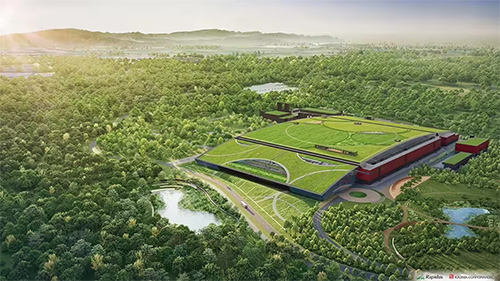
Founded in August 2022 with joint investment from eight major Japanese industrial giants including Toyota, Sony, SoftBank and Fujitsu, the firm has completed trial fabrication and test wafer runs of 2nm Gate-All-Around (GAA) transistors at its IIM-1 fab in Chitose, Hokkaido.
According to Rapidus, its target pricing for 2nm wafer foundry services ranges from JPY 3 million to JPY 3.5 million per wafer (equivalent to approximately RMB 126,000 to RMB 147,000 at current exchange rates). Atsuyoshi Koike, CEO of Rapidus, explicitly stated that the company will adopt a pricing strategy that “cannot be outmatched by TSMC.”
Currently, TSMC quotes roughly USD 30,000 for 300mm wafers on comparable advanced process nodes, with reports of further price hikes previously circulating. If Rapidus delivers on its targeted pricing, it will hold clear cost competitiveness.
Rapidus has secured tangible progress in customer acquisition. Fujitsu, one of its founding investors, has been confirmed as the first commercial customer and plans to entrust Rapidus with manufacturing its 2nm AI neural network processors. IBM Japan is viewed as the second anchor customer, and the two parties are evaluating advanced semiconductor production via Rapidus’s foundry services. In addition, Canadian AI chip startup Tenstorrent has secured early capacity reservations. Per Koike’s disclosure, Rapidus has engaged with more than 60 prospective clients since the start of 2026.
Government financial backing for Rapidus continues to expand. On April 11, 2026, Japan’s Ministry of Economy, Trade and Industry (METI) announced an additional JPY 631.5 billion in R&D subsidies for fiscal 2026 (around RMB 26.492 billion at current exchange rates). This brings cumulative government R&D support for Rapidus to approximately JPY 2.354 trillion (roughly RMB 98.753 billion). Combined with JPY 167.6 billion raised from 32 private enterprises in February 2026 (approximately RMB 7.031 billion) and a planned additional JPY 150 billion in private investment (around RMB 6.293 billion), total capital injection into Rapidus is projected to approach JPY 3 trillion (approximately RMB 125.853 billion) by fiscal 2027.
Rapidus intends to start manufacturing 2nm test chips for clients by the end of 2026. Its Chitose facility will launch with an initial monthly capacity of 6,000 wafers, with a target to scale up to roughly 25,000 wafers per month by 2028.
Technologically, Rapidus will not stop at the 2nm node. The company plans to fully kick off R&D for the 1.4nm process in 2026, targeting mass production in 2029. Looking further ahead to the 1nm node, Kazunari Ishimaru, Chief Technology Officer of Rapidus, stated the firm aims to narrow its development lag behind TSMC to around six months. Rapidus will sustain deep collaboration with IBM, with half of its engineering team stationed in New York, USA, to conduct joint research and development.
(Reprinted from https://news.eccn.com/)