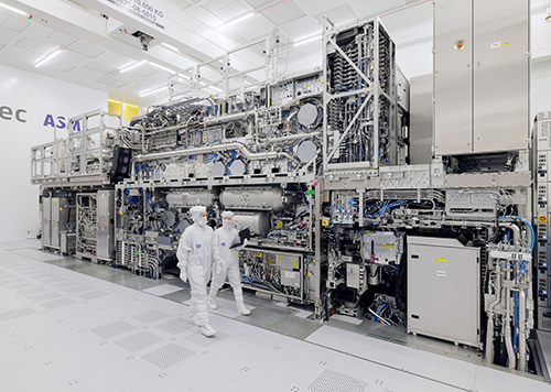
On November 19, ASML, a leading lithography equipment manufacturer, held a media briefing in Taiwan, China. Hsu Kuan-cheng, ASML’s Customer Marketing Director for Taiwan (China) and Southeast Asia, stated that as semiconductor process technology continues to shrink, High NA EUV lithography machines will help customers save time and costs. Currently, major customers include Intel, IBM, and Samsung, with a cumulative total of over 350,000 wafers exposed using High NA EUV lithography equipment.
Hsu noted that today’s society is shifting from "chips everywhere" to "AI everywhere." AI will drive growth in demand for both advanced and mature semiconductor processes, and global semiconductor sales are expected to exceed $1 trillion by 2030.
While extending Moore’s Law poses challenges, the law will continue to guide development over the next 10 to 15 years, with semiconductor process technology continuing to shrink. Hsu recalled that the industry once raised doubts when transitioning from immersion lithography to Extreme Ultraviolet (EUV) lithography, and High NA EUV is now facing similar skepticism.
The "doubts" Hsu referred to mainly stem from industry concerns that High NA EUV is overly expensive, and the benefits from its deployment will be disproportionate to the investment.
Previously, Zhang Xiaoqiang, Senior Vice President of Business Development and Global Sales at TSMC, publicly stated that while impressed by High NA EUV’s capabilities, the equipment price exceeds 350 million euros ($378 million). Current standard EUV lithography machines will continue to support TSMC’s cutting-edge process production until 2026, and the advanced A16 process will also use standard EUV equipment. Later, at TSMC’s Technology Forum Europe held in Amsterdam, the Netherlands, Zhang reaffirmed TSMC’s long-term stance on High NA EUV: the company will not adopt High NA EUV for its A16 (1.6nm-class) and A14 (1.4nm-class) process technologies.
In response, Hsu emphasized that High NA EUV equipment offers higher imaging quality and process simplification advantages, which help customers save time and costs.
According to Hsu, ASML’s current High NA EUV customers include Intel, IBM, and Samsung, with over 350,000 wafers processed using the technology to date. However, on September 3 this year, SK hynix announced that it had installed and put into mass production its first High NA EUV (High Numerical Aperture Extreme Ultraviolet Lithography) system at its M16 manufacturing plant in Icheon, South Korea.
In addition to High NA EUV targeting cutting-edge processes, ASML continues to optimize Deep Ultraviolet (DUV) lithography equipment to help customers meet large-scale DUV exposure needs at lower costs. Furthermore, ASML has launched the XT:260 to support advanced packaging applications.
(Reprinted from https://news.eccn.com/)