Citing industry insiders, The Korea Economic Daily reported that amid surging demand for AI-related chips, Samsung Electronics is further beefing up its industrial chain layout and plans to build a state-of-the-art semiconductor packaging factory in Gwangju, South Korea.
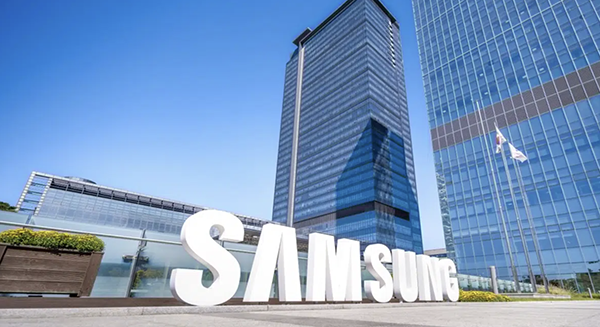
The investment scheme is expected to be unveiled during the presidential roundtable scheduled for June 29. The meeting will center on South Korea’s strategic shift for future economic growth, with attendees including Samsung Group Chairman Lee Jae-yong and SK Group Chairman Choi Taewon. Samsung declined to comment on the reports, while the South Korean Presidential Office stated that corporate investment decisions remain at each company’s sole discretion.
Against the rapid evolution of the AI semiconductor supply chain, advanced packaging has emerged as one of the pivotal links determining chip performance and market competitiveness. If the project moves forward, it will mark Samsung’s continued heavy investment in advanced packaging. The company is already ramping up spending on the HBM market in a bid to challenge industry leader SK Hynix’s dominant position. Samsung Electronics’ client roster already covers major AI players including NVIDIA, AMD and Google. In May this year, Samsung announced it had begun supplying samples of its latest 12-layer HBM4E memory to customers, demonstrating its accelerated push to compete in next-generation AI memory products.
(Reprinted from https://news.eccn.com/)