On October 6 (local time), imec (Interuniversity Microelectronics Centre), the world’s leading research and innovation hub for nanoelectronics and digital technologies, announced that it has welcomed AIXTRON, GlobalFoundries, KLA Corporation, Synopsys, and Veeco as the first partners of its open innovation program track for 300mm gallium nitride (GaN) power electronics applications in both low-voltage and high-voltage segments.
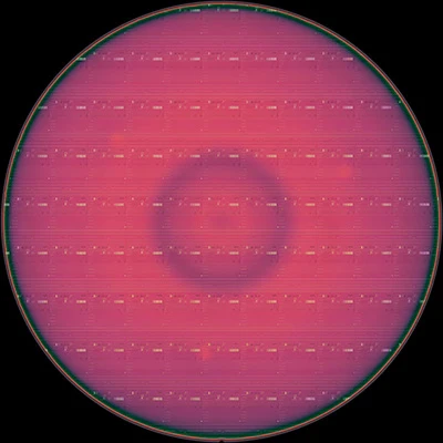
△ 300mm GaN-on-Si wafers from AIXTRON, after p-GaN etching at imec, are inspected on KLA’s Series 8/CIRCL™ tools.
According to introductions, this project is part of imec’s Industrial Affiliation Program (IIAP) for GaN power electronics. It aims to develop 300mm GaN epitaxial growth processes and manufacturing flows for low-voltage and high-voltage GaN high-electron-mobility transistors (HEMTs). The use of 300mm substrates not only reduces the manufacturing cost of GaN devices but also enables the development of more advanced power electronic components—such as high-efficiency low-voltage point-of-load converters for CPUs and GPUs.
Recently launched GaN-based fast battery chargers in the market have highlighted the potential of GaN technology in power electronics applications. Supported by continuous progress in GaN epitaxial growth, GaN device and integrated circuit manufacturing, reliability and robustness, and system-level optimization, GaN technology is expected to enable a new generation of power electronic products. Compared with silicon-based solutions, these products will enter the market with smaller form factors, lighter weights, and superior energy conversion efficiency. Examples include on-board chargers and DC/DC converters for automotive applications, inverters for solar panels, and power distribution systems for telecommunications and AI data centers—GaN-based building blocks contribute to the overall decarbonization, electrification, and digitalization of society.
A notable trend in GaN technology development is the shift toward larger wafer diameters, which are currently mostly 200mm. Building on its 200mm expertise, imec is taking the next step by launching the 300mm GaN project. Stefaan Decoutere, Researcher and Program Director of imec’s GaN Power Electronics Program, stated: “The benefits of transitioning to 300mm wafers go beyond scaling up production and reducing manufacturing costs. Our CMOS-compatible GaN technology can now leverage state-of-the-art 300mm equipment, which will allow us to develop more advanced GaN-based power devices. For instance, aggressively scaled low-voltage p-GaN gate HEMTs for point-of-load converters, enabling energy-efficient power delivery for CPUs and GPUs.”
As part of the 300mm GaN program, 300mm silicon will first be used as the substrate to establish a baseline lateral p-GaN HEMT technology platform for low-voltage applications (100V and above). To this end, process module work centered on p-GaN etching and ohmic contact formation is underway. Later, high-voltage applications will become the focus. For 650V and above, development will use 300mm half-spec and CMOS-compatible QST® engineered substrates (a material with a polycrystalline AlN core). During the development process, control of 300mm wafer bow and mechanical strength is a top priority.
The 300mm GaN program follows successful 300mm wafer processing tests and mask set development. imec expects to have a complete 300mm GaN production line installed in its cleanroom by the end of 2025. Stefaan Decoutere added: “The success of 300mm GaN development also depends on our ability to build a strong ecosystem and collectively drive innovation from 300mm GaN growth and process integration to packaging solutions. Therefore, we are pleased to announce AIXTRON, GlobalFoundries, KLA Corporation, Synopsys, and Veeco as the first partners of our 300mm GaN open R&D program, and we look forward to welcoming more partners soon. Because developing advanced GaN power electronics requires tight coupling between design, epitaxy, process integration, and applications—a coupling that proved crucial for our pioneering work in 200mm GaN.”
(Reprinted from https://news.eccn.com/)