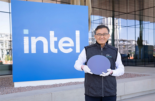
A report released by analysts at Wall Street investment firm KeyBanc following their recent Asia tour notes that Intel Foundry is demonstrating an extremely strong growth momentum. According to the latest survey, Intel is poised to capture a large volume of orders from multiple hyperscale AI and cloud providers, primarily for its advanced 14A and 18A-P process nodes, with orders on the 14A node accounting for the largest share.
KeyBanc stated in the report that Intel has secured foundry contracts with multiple major technology companies, including network switches for Broadcom, server CPUs for Google and Microsoft, gaming GPUs for NVIDIA, as well as orders from AMD. In addition, Intel has won a multi-year, multi-series chip contract with Apple. Intel will manufacture Apple’s M-series and A-series chips using its 14A process. This development dispels prior market rumors that Apple would adopt the 18A-P process, yet it has also drawn pushback from some professionals in the semiconductor industry.
Beyond signed customers, potential clients including Anthropic, Amazon, and SpaceX/Tesla Terafab are evaluating Intel’s 18A-P and 14A processes, with most evaluators showing preference for the 14A node.
Intel’s 14A process is a 1.4nm-class wafer manufacturing technology featuring two core technological breakthroughs:
PowerDirect Backside Power Delivery technology, which shifts power lines entirely to the backside of the silicon wafer, freeing up front-side space for data signal transmission to reduce resistance and boost transistor density.
RibbonFET 2 transistors and the second-generation Gate-All-Around (GAA) architecture, delivering tighter electrostatic control for miniaturized transistors, increasing drive current and minimizing voltage leakage.
On the financial front, KeyBanc estimates Apple alone will have a wafer start volume of 600,000 wafers on the 14A process, with potential revenue contribution ranging from USD 15 billion to USD 20 billion. Meanwhile, the custom ASIC chips commissioned by Anthropic are projected to hit 5 to 10 million units. When advanced packaging is factored in, the associated potential revenue could reach USD 40 billion to USD 80 billion.
In addition to advanced process nodes, Intel holds strong influence in advanced packaging. Intel’s EMIB technology interconnects chiplets via silicon bridges embedded in organic substrates. The upgraded EMIB-T further incorporates Through-Silicon Via (TSV) technology, enabling vertical transmission of power and high-speed signals to realize 3D chip stacking.
KeyBanc forecasts that Intel’s production of 5 to 6 million units of Google’s Humufish TPUv9 and Icefish TPUv10 packaged with EMIB-T will generate USD 1.2 billion to USD 1.5 billion in revenue. Packaging for Qualcomm’s AI300 ASIC (approximately 1 million units) may contribute an additional USD 2 billion to USD 3 billion. Moreover, Intel’s EMIB-M packaging technology is expected to drive business through orders for Amazon Trainium 3 and Microsoft Cobalt 400.
In terms of supply chain, EMIB-T substrate partners include Ibiden (the primary anchor supplier), Shinko, UMTC and AT&S, adopting Ajinomoto Build-up Film (ABF) as the laminated dielectric material. Currently, Ibiden averages a yield rate of roughly 50% to 60% for EMIB-T substrates, while UMTC’s yield stands at only 20% to 30%. This may constrain capacity ramp-up for Google’s “Humufish” to the target of 5 to 6 million units. Even so, UBS anticipates Intel’s EMIB-T will support more than 2 million substrates by 2028 to meet demand from MediaTek’s collaboration with Google on next-generation TPU v9 chips “Humufish” and “Triggerfish”.
Market sources also indicate that NVIDIA may adopt Intel’s Foveros packaging technology in 2028. Foveros leverages Copper-to-Copper Hybrid Bonding to deliver true 3D active chip stacking, offering ultra-high interconnect density and extremely low signal latency. Should NVIDIA’s adoption materialize, it will become a major growth driver for Intel in the years ahead.
(Reprinted from https://news.eccn.com/)