Intel Foundry has recently released full details of EMIB-T, the latest iteration of its advanced Embedded Multi-Die Interconnect Bridge (EMIB) packaging technology. Developed to address the massive power and data transmission requirements of next-generation AI processors and data center hardware, this technology optimizes chiplet architectures and eliminates the need for manufacturing oversized monolithic dies.
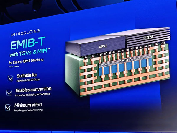
Intel unveiled its new suite of 2.5D advanced packaging technologies at the Intel Foundry Summit last April, including EMIB-T tailored for future high-bandwidth memory applications. It marks the first EMIB implementation that uses TSVs to route signals through the bridge, rather than around it, and is primarily designed for die-to-HBM4 interconnection.
Industry sources revealed in early May that MediaTek will adopt Intel’s EMIB-T packaging technology for its new TPU codenamed "Humufish", which is being developed for Google and scheduled to launch in the second half of 2027. The technology has achieved a yield rate of 90% during validation.
Intel further explained that traditional multi-die packaging generally relies on large, costly silicon interposers covering the entire base of processor chips for underlying interconnection. By contrast, EMIB-T eliminates bulky silicon substrates and deploys compact high-speed silicon bridges at designated positions to connect adjacent chips for signal transmission.
Engineers at Intel’s Fab 9 wafer fabrication facility in New Mexico have successfully embedded chips directly onto silicon bridges, enabling direct cross-bridge communication between neighboring data center chips. The innovation delivers substantial material cost savings, faster electrical response and shorter cycle time for high-speed inter-chip communication.
Intel highlighted that EMIB-T’s core advancement lies in routing traces directly through the silicon bridge. In previous generations, power had to bypass the interconnect bridge, which caused resistance and slowed down signal delivery. With power and signals traveling straight through the bridge into silicon components, power loss is greatly minimized and signal transmission speed is maximized. This upgrade is critical for modern High-Bandwidth Memory (HBM), which demands steady power supply and ultra-fast signal cycles to deliver superior responsiveness.
As a core technology for Intel Foundry to integrate heterogeneous chiplets, EMIB-T enables the packaging of chiplets from diverse sources into industry-leading large-scale integrated devices. Compared with conventional full-size silicon interposers, EMIB-T improves production yield and cuts costs, and also makes it feasible to develop ultra-large side-by-side AI processors for data center deployments.
(Reprinted from https://news.eccn.com/)