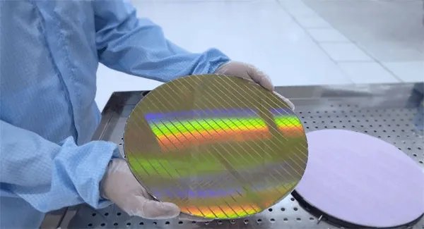
According to a report by Taiwanese media DigiTimes, in order to compete with TSMC’s 2nm (N2) process, Samsung has cut the foundry price of its 2nm (SF2) process wafers to $20,000—one-third lower than the rumored $30,000 foundry price of TSMC’s 2nm wafers.
This move is clearly aggressive for Samsung, but it may also be necessary. Without adoption by major customers, relying solely on the demand for Samsung’s own next-generation flagship Exynos processors would be insufficient to achieve reasonable capacity utilization at its 2nm fabs. If most of the capacity remains underutilized, Samsung will also face huge losses.
Earlier information indicates that Samsung’s initial yield rate for the 2nm process was below 30%, but the company is fully committed to improving yields, with the goal of raising the 2nm yield rate to 70% by the end of the year.
In early September, South Korean media ETnews quoted industry insiders as reporting that Samsung Electronics’ Foundry Division is preparing for mass production of the next-generation flagship mobile processor Exynos 2600, which is expected to use Samsung’s own 2nm process. This seems to imply that Samsung is about to resolve its yield issues.
In addition, leading electric vehicle manufacturer Tesla signed a semiconductor foundry contract worth up to 22 trillion won (approximately $16.5 billion) with Samsung last month. The focus of this cooperation is to produce high-performance system semiconductors named "AI6" for Tesla. These chips are expected to be mass-produced using Samsung’s second-generation 2nm (SF2P) process at Samsung’s U.S. fab in 2026, and will be widely used in Tesla’s next-generation Full Self-Driving (FSD) systems, robots, and data centers. With Tesla’s support, the yield rate of Samsung’s SF2P process is expected to be further improved.
However, currently, apart from the previously revealed Exynos 2600, Samsung’s first-generation 2nm process has not yet been adopted by other major customers.
In contrast, TSMC’s 2nm process has not yet entered mass production, and rumors suggest its foundry price will be as high as $30,000. Even so, TSMC has already secured major customers such as Apple, AMD, Qualcomm, and MediaTek. Additionally, Broadcom and some ASIC customers (such as Google and Amazon) may also adopt the process.
Ahmad Khan, President of the Semiconductor Products and Solutions Division at KLA—a leading U.S. semiconductor equipment company—recently stated at an event organized by Goldman Sachs that TSMC’s 2nm process has now gained 15 customers, 10 of which are for HPC (High-Performance Computing) applications, and the rest are likely mobile chip customers.
Therefore, for Samsung, since its 2nm process cannot compete with TSMC in terms of performance and yield rate, cutting prices may be the only way to attract other customers.
DigiTimes also commented that Samsung’s foundry has a track record of price competition. Given that TSMC’s current and future fabs are operating at full capacity and commanding corresponding premiums, Samsung’s $20,000 price tag for 2nm wafers is undoubtedly an attractive option for customers who cannot or are unwilling to pay TSMC’s asking price.
(Reprinted from https://news.eccn.com/)