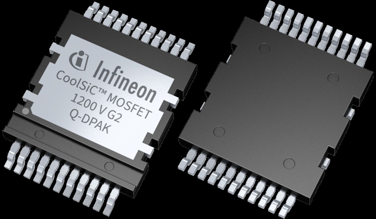
SiC MOSFET 1200 V G2 in a top-ventilated Q-DPAK package. This new semiconductor device offers superior thermal performance, system efficiency, and power density, designed to meet the demanding performance and reliability requirements of industrial applications such as electric vehicle chargers, photovoltaic inverters, UPS, motor drives, and solid-state breakers, among others.
The CoolSiC 1200 V G2 technology offers significant improvements over the previous generation, reducing switch losses by up to 25% and increasing system efficiency by 0.1% while maintaining the same drain-source resistance (Rds(on)). Based on Infineon's advanced .XT diffusion bonding technology, the thermal resistance of the G2 family is reduced by more than 15% compared to the G1 family, and the MOSFET temperature is also reduced by 11%. With excellent drain-source resistance (Rds(on)) of 4 mΩ to 78 mΩ and a comprehensive product portfolio, designers can flexibly select products to improve system performance and meet the requirements of target applications. Additionally, the new technology supports overload operation at junction temperatures (Tvj) up to 200°C and has excellent anti-parasitic conduction capabilities, ensuring reliable operation in dynamic and demanding operating conditions.
The Infineon CoolSiC MOSFET 1200 V G2 is available in two Q-DPAK packages, a single switch and a dual half-bridge. Both variants belong to Infineon's broader X-DPAK top side cooling platform. The package thickness is unified at 2.3 mm for all top side cooling (TSC) versions (including Q-DPAK and TOLT), providing a high degree of design flexibility that allows customers to flexibly extend and combine different products under a single thermal solution. This design flexibility simplifies the development of advanced power systems and facilitates customer customization and extension of their solutions as required.
Q-DPAK packaging significantly enhances thermal performance by achieving direct thermal conductivity between the device top and the heat sink. Compared to traditional bottom-side cooling packages, this direct thermal path significantly improves thermal conductivity efficiency, allowing for more compact system designs. Additionally, the layout design of the Q-DPAK packaging greatly reduces parasitic inductance, which is crucial for improving switch speed, thereby enhancing system efficiency and reducing the risk of voltage overshoot. The compact footprint of this packaging makes it suitable for applications with space constraints, and its compatibility with automated assembly processes simplifies the manufacturing process, ensuring cost-effectiveness and scalability.
(Reprinted from https://www.eefocus.com)